Through Hole Assembly

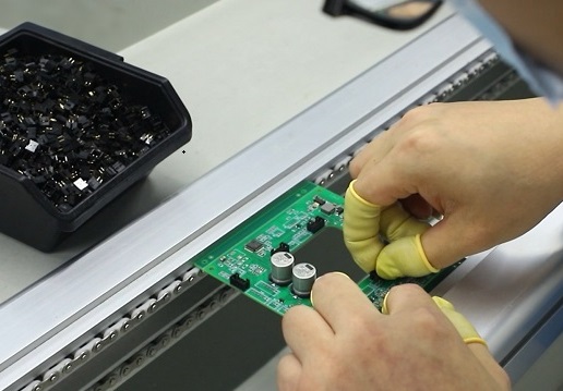
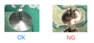
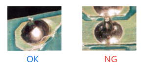
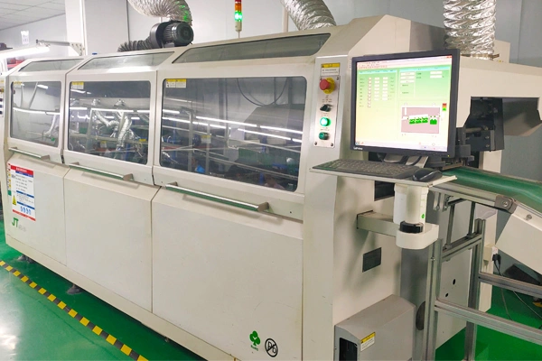
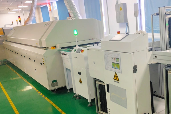
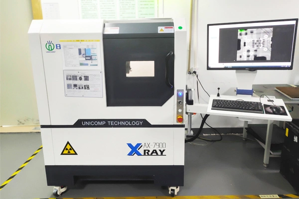
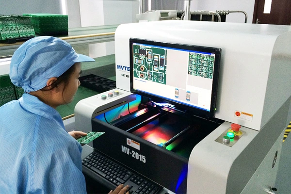
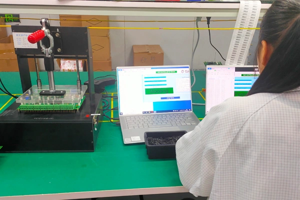
Through-hole PCB assembly is a method of attaching components to printed circuit boards. It involves inserting component leads through pre-drilled holes in the PCB, which creates strong connections between parts and the board. OurPCB offers expert through-hole PCB assembly services for reliable electronic products.


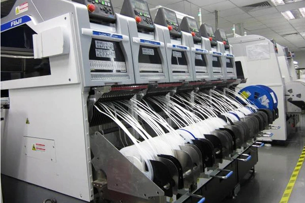
PCB through-hole assembly involves inserting components with leads through holes in a printed circuit board (PCB) and soldering them on the opposite side.

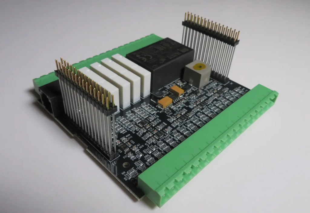
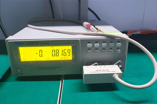
Through-hole PCB assembly works well for larger components and high-stress applications. It’s often used for power supplies, connectors, and specialized parts. Through-hole assembly provides strong mechanical bonds, which makes it ideal for products that may face physical stress or vibration.

The Benefits of Partnering with JinTeng as Your Through Hole PCB Assembly Suppliers

JinTeng offers top-quality through-hole PCB assembly services. We combine skilled technicians with advanced equipment to deliver reliable results. Our focus on precision and efficiency sets us apart in the industry.

Expert Technicians

Advanced Equipment

Quality Control

Flexible Solutions

Why Choose Through Hole PCB Assembly Manufacturers?

Through-hole PCB assembly machine services offer unique advantages for certain projects. It’s ideal for products that need durability and easy repairs. Choosing a specialized manufacturer ensures you get the best results for your specific needs.

Durability

Ease of Repair

Compatibility

Reliability

Technical Capabilities

JinTeng’s through-hole PCB assembly factory equipment is top-of-the-line. We use advanced insertion machines for accurate component placement. Our soldering techniques ensure strong, reliable connections, and we can handle boards of various sizes and complexities. Our facility is equipped with capabilities to manage both prototype and high-volume production runs efficiently.

Capabilities & Services

* THT Assembly Standard of Criterion in PCBbee

1. Short Circuit

Features: The solder on the pad is connected between two or more adjacent solder joints on different circuits.

Acceptance Standard: If there is no such phenomenon, it is accepted. If it is found, secondary repair welding is required.

Impact: Seriously affects the electrical characteristics and causes serious damage to components.

2. Open Solder

Features: The components’ pins are not covered with solder
Acceptance standard: If there is no such phenomenon, it is accepted. If it is found, secondary repair welding is required.
Impact: The circuit can not be conducted, the electrical function can not be shown, and occasionally poor welding and electrical tests can not be detected.

3. Components Pin Too Long

Features: The components’ pins are not covered with solder
Acceptance standard: If there is no such phenomenon, it is accepted. If it is found, secondary repair welding is required.
Impact: The circuit can not be conducted, the electrical function can not be shown, and occasionally poor welding and electrical tests can not be detected.

4. Cold Solder

Features: The solder joint has an unsmooth appearance. In severe cases, it will wrinkle or crack around the pin.
Acceptance standard: If there is no such phenomenon, it is accepted. If it is found, secondary repair welding is required.
Influence: Solder joint reliability time is short, easy to begin to have poor welding phenomenon after being used for a period of time, leading to functional failure.

5. Pinhole

Features: Pinholes are on the surface of the solder joint.
Acceptance standard: If there is no such phenomenon, it is accepted. If it is found, secondary repair welding is required.
Influence: Poor appearance and poor solder joint strength.

What we factory

Electronic Manufacturing Factory

Item 1
Item 2
Item 3
Item 4
Item 5
Item 6
Item 1
Item 2
Item 3
Item 4
Item 5
Item 6