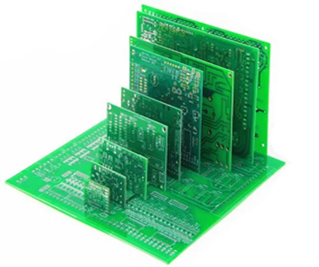
PCB Manufacturing Services
One-stop China PCB Manufacturer
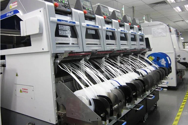
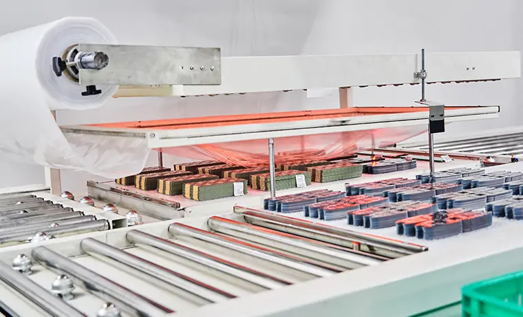
JINTENG provides professional PCB assembly services with precision and reliability. Based in China, we deliver high-quality PCB assembly directly to customers in the USA and across the globe. Our end-to-end solutions include component sourcing, SMT, and through-hole assembly, ensuring efficient production and consistent quality from a single trusted PCB manufacturer.
We also specialize in circuit card assembly solutions, ensuring all your components are properly placed and connected for optimal performance. Whether you’re working with HDI PCBs or need specialized testing such as In-Circuit Testing for PCBs, our services provide you with a one-stop solution for all your needs.
For more advanced applications, we also offer selective gold plating processes to enhance your PCB’s performance in sensitive areas that require high conductivity and corrosion resistance. Additionally, effective PCB Thermal Management is crucial for maintaining component reliability and preventing overheating in high-performance electronic assemblies.
PCB Manufacturing Materials
FR4
A common fiberglass-reinforced epoxy laminate, known for its durability and electrical insulating properties.
CEM-1 and CEM-3
Composite materials offering cost-effective alternatives for less demanding applications.
Flexible Materials
Such as polyimide, used for creating bendable and foldable PCBs.
High-Frequency Materials
Designed for applications requiring minimal signal loss and high-speed data transmission.
JinTeng Custom PCB Manufacturing & Assembly Services
Flexible PCB Manufacturer
Rogers PCB Manufacturer
Aluminum PCB Manufacturer
Metal Core PCB Supplier
High Tg PCB Manufacturer
High Frequency PCB Manufacturer
Heavy Copper PCB Manufacturer
China PCB Manufacturer
Types of Circuit Boards
PCB Materials
Rogers PCB
Ceramic PCB
Teflon PCB
Heavy Copper PCB
Standard PCB Thickness
High Tg PCB
Halogen-Free PCB
High Frequency PCB
High Speed PCB Manufacturer
High-Speed PCB Design
Controlled Impedance PCB
Blind Via PCB
IC Substrate
Controlled Impedance PCB
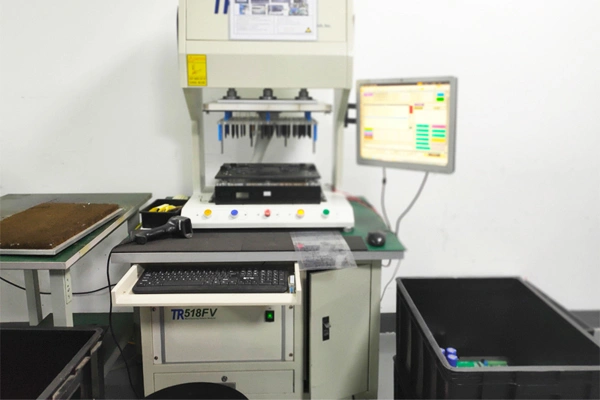
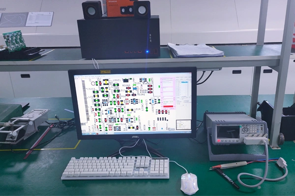
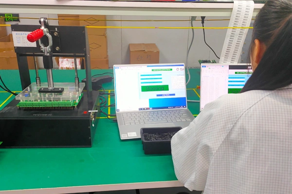
AOI Testing
PCBA Testing
Inverter PCBs
Radar PCBs
Medical PCBs
LED PCBs
Embedded PCBs
Signal Integrity Solutions
BT PCB Manufacturer
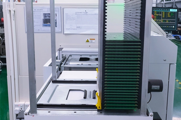
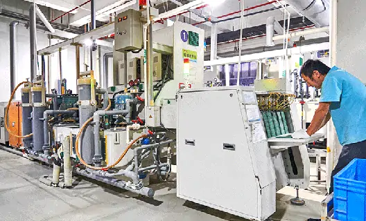
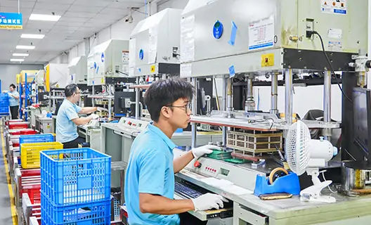
Key PCB Manufacturing Processes
01 File Review
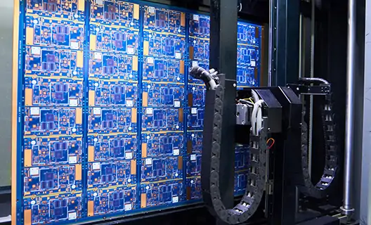
02 Inner Layer Fabrication
03 Drilling
04 Through-Hole Plating
05 Outer Layer Fabrication
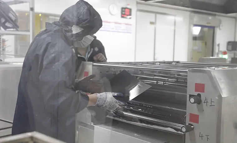
06 Solder Mask Application
07 Surface Finish
08 Electrical Testing
09 Final Inspection
10 Packaging
PCB Manufacturing Capabilities
General Parameters
| Manufacturing Materials | Capability |
|---|---|
| FR4 | Tg 135: KB6160, S1141 Tg 150: KB6165, S1000H Tg 170: KB6167, S1000-2M, IT180A, TU768 |
| Halogen Free FR4 | Tg 150: S1150G Tg 170: S1165, TU862HF |
| Ceramic Filling High Frequency Material | Rogers 4003C/4350B |
| PTFE High Frequency Material | Rogers Series, Arlon Series, Taconic Series, F4BM Series |
| Special PP | NFPP: Arlon 49 N, VT47 Ceramic Filling PP: Rogers 4450F PTFE PP: Arlon 6700, Taconic FR-27 |
| Rigid PI Material | Arlon 85 N, VT901 |
| Metal Base Board | Bergquist Al base, Chinese Brand Al base, Copper base |
| Material Mixed Laminate | 4 layers – 10 layers (FR4 + Ro4350, FR4 + Aluminium, FR4 + FPC) |
| Note | Other special materials can be processed and produced by means of customer supply or purchasing. |
| Item | Standard | Advanced | Innovative |
|---|---|---|---|
| IC Space (Green Color) | 4 | 4 | 3 |
| IC Space (Other Color) | 5 | 5 | 4 (blue oil) |
| Liquid Photoimageable (LPI) Solder Mask Registration | 3mil | 2mil | 1.5mil |
| Thickness T>1.0 mm | ±10% | ±10% | ±8% |
| Tolerance T≤1.0 mm | ±0.1 | ±0.1 | ±0.1 |
| Board Thickness (mm) | 0.5-5.0 | 0.4-6.5 | 0.25-10 |
| Hole Aspect Ratio | 10:01 | 12:01 | 20:01 |
| Via Size For Plug Solder Mask | 0.25-0.5 | 0.20-0.5 | 0.15-0.6 |
| Via Size For Plug Resin And Capped Copper | 0.25-0.5 | 0.20-0.5 | 0.075-0.6 |
| Panel Size (mm) | 457×609 | 457×609 | 600×1000 |
| Bow And Twist | ≤0.75% | ≤0.75% | ≤0.5% |
Inner Graphics
| Item | Basic copper thickness | Line Width/Space |
Minimum inner line width distance | 1/3 OZ | 2.7/2.7 |
| 0.5 OZ | 3/3 | |
| 1.0 OZ | 3.5/3.5 | |
| 2.0 OZ | 5/5.5 | |
| 3.0 OZ | 6/7.5 | |
| 4.0 OZ | 7/11.5 | |
| 5.0 OZ | 10/16 | |
| 6.0 OZ | 10/10.5 | |
| 10 OZ | 18/20 | |
| 12 OZ | 22/24 | |
Hole to Line Spacing | 4 layers | ≥6mil(1 core) |
| 6 layers | ≥7mil(2 core) | |
| 8 layers | ≥7mil(3 core) | |
| 10 layers and above | ≥8mil | |
| Line Width/Space Accuracy | Non-impedance plate ±20%; Impedance plate ±10% | |
| Alignment accuracy | ±25um(CCD) | |
Outer Graphics
| Item | Basic copper thickness | Line Width/Space |
Minimum outer line (mil) | 1/3 OZ | 3/3 |
| 0.5 OZ | 3.5/3.6 | |
| 1.0 OZ | 4/4.4 | |
| 2.0 OZ | 5/5.5 | |
| 3.0 OZ | 6/7.5 | |
| 4.0 OZ | 14/12 | |
| 5.0 OZ | 18/17 | |
| 6.0 OZ | 13/11 | |
| 10 OZ | 16/26 | |
| 12 OZ | 24/32 | |
The minimum line width of the outer etched word | Base Copper H OZ; 8mil | |
| Base Copper 1 OZ; 10mil | ||
| Base Copper 2 OZ; 12mil | ||
| Line Width/Space Accuracy | Non-impedance plate ±20%; Impedance plate ±10% | |
| Alignment accuracy | ≤24um(LDI) | |
Hole Processing
| Item | Mass Production | Prototyping | |
Through Hole | Hole Diameter (max) | 6.5mm, thickness <6.4mm | Greater than 6.5mm (hole expansion process) |
| Hole Diameter (min) | 0.15mm,thickness<1.0mm | 0.15mm, thickness<1.6mm | |
| Hole tolerance | NPTH±0.05mm, PTH hole±0.075mm, crimping hole±0.05mm | ||
| Hole tolerance | ±0.05mm | ||
| Thickness ratio | 8:01 | 20:01 | |
| Minimum Hole Spacing | The same grid > 8mil; non-same grid ≥ 12mil | The same grid ≥ 6mil, not the same grid ≥ 10mil | |
Deep Hole Control | Minimum depth control hole diameter | 0.155mm | |
| Depth Control Accuracy | 0.1mm | 0.05mm | |
| Hole Depth Thickness Diameter Ratio | ≤0.6:1 | ≤0.8:1 | |
| Control depth groove depth tolerance | ±0.15mm | ±0.1mm | |
Stepped Hole | Step hole diameter tolerance | 0.1mm | 0.05mm |
| Step hole depth tolerance | 0.2mm | 0.1mm | |
Laser Hole | Laser Hole Copper | ≥10um | |
| Hole Diameter range | 0.1mm-0.15mm | 0.076mm-0.15mm | |
| Laser blind hole thickness to diameter ratio | ≤0.6:1 | ≤0.8:1 | |
| Outer line width and line spacing | 3.5/4mil | 3.5/3.5mil | |
| Inner line width and line spacing | 3.0/3.5mil | 3.0/3.3mil | |
| Laser Blind Hole Medium Thickness | 2.5-4mil | 2.5-5mil | |
Back Drilling | Depth Tolerance | ±0.1mm | |
| Position Tolerance | ±0.1mm | ||
| Hole to outer line distance | ≥0.15mm | ≥0.125mm | |
| Hole to inner line distance | ≥0.175mm | ≥0.15mm | |
Countersunk Hole | Countersunk drill diameter | The 45° countersunk bit has a diameter of 4.5mm | |
| 60°, 82°, 90° countersunk bit diameter is 6.35mm | |||
| 100° countersunk bit diameter is 6.5mm | |||
| Outer Aperture Accuracy | ±0.2mm | ||
| PTH Countersunk Ring Width | 8mil | ||
| PTH countersunk hole distance line | 12mil | ||
Conical Hole | Opening Tolerance | ±0.2mm | |
| Aperture angle | 45°、60°、90° | ||
| Slot | Minimum Slot | 0.5mm | |
Outline
| Item | Mass Production | Prototyping | |
V-CUT | Angle | 20°、30°、45°、60° | |
| Jumping Knife Distance | ≥8 mm | ||
| Board Thickness | 0.4 mm-3.0mm | ||
| Thickness accuracy | ±0.1 mm | ±0.05 mm | |
Gong Board | Minimum gong cutter diameter | 0.6 mm | |
| Control deep gong plate thickness | ≥0.4 mm | ||
| Depth tolerance of deep gong plate | ±0.15 mm | ±0.1 mm | |
| Tolerance of deep gong plate size | ±0.13 mm | ||
Hypotenuse | The outer layer of the top of the gold finger is copper | Bevel depth +0.2 mm | |
| The inner layer of the top of the gold finger is copper | Bevel depth +0.4 mm | ||
| Angle (tolerance ±5°) | 20°, 30°, 45°, hypotenuse angle is usually 30° | ||
Surface Treatment
| Item | Standard | Advanced | Innovative | |
ENIG | Nickel Thickness (um) | 2.0-5.0 | 3.0-5.0 | 3.8-7.62 |
| Gold Thickness(uinch) | 1.0-2.0 | 2.0-3.0 | 3.0-5.0 | |
Hard Gold (Au Thickness) | Normal Golden Finger(um) | 0.15 | 0.8 | 3.0 |
| Selective Hard Gold (um) | 0.15 | 0.8 | 2.0 | |
ENEPIG | Nickel Thickness (um) | 2.0-5.0 | ||
| Palladium Thickness(uinch) | 4.0-20.0 | |||
| Gold Thickness(uinch) | 1.0-5.0 | |||
Plating Gold | Nickel Thickness (um) | 2.0-7.62 | ||
| Gold Thickness(uinch) | 1.0-5.0 | |||
| Immersion Tin | Tin Thickness (um) | 0.8-1.2 | ||
| Immersion Silver | Sliver Thickness (um) | 0.15-0.4 | ||
| OSP (um) | 0.2-0.6 | |||
| Tin Lead HASL (um) | 2.0-40.0 | |||
| Lead Free HASL (um) | 2.0-40.0 | |||
| Note:Tin Lead /LF HASL panel size should less than ≤500×600 mm,thickness≥0.6 mm;Hard Gold panel size≤400×500 mm,the other surface treatment panel size less than 500×900 mm | ||||
Special Process
| Item | Standard | Advanced | Innovative |
|---|---|---|---|
| Back Drilling | YES | YES | YES |
| Heavy Copper PCB with Blind/Burried Via | YES | YES | YES |
| Step Slots | YES | YES | YES |
| POFV | YES | YES | YES |
| Plated Half Holes/Edge Plating | YES | YES | YES |
| Hybrid Material Lamination | YES | YES | YES |
Delivery Ability
| 1-2L Lead-time | Sample Expedited 24 hours and 48 hours, Normal2-5 days, Mass production 5-7days |
| 4- 8L Lead-time | Sample Expedited 48 hours 72 hours, Normal 5-7days,Mass production 7-10 days |
| 10-18L Lead-time | 10-15 days,Special circumstances based on the actual PCB design |
| More than 20L Lead-time | 15-20 days ,Special circumstances based on the actual PCB design |
| Acceptable File Format | ALL Gerber Files、POWERPCB、PROTEL、PADS2000、CAD、AUTOCAD、ORCAD、P-CAD、CAM-350、CAM2000 etc. |
PCB Manufacturing FAQs
What are the costs associated with custom PCB manufacturing?
- PCB Size and Layers: Larger and more layered boards generally cost more.
- Material Choice: High-performance materials such as FR4, aluminum, or flex materials can affect pricing.
- Order Volume: Bulk orders are eligible for significant discounts.
- Special Requirements: Features like HDI, blind/buried vias, or impedance control may incur additional costs.
- Assembly Services: Turnkey assembly, component sourcing, and other add-ons contribute to the total cost.
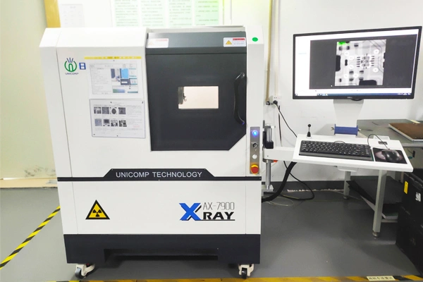
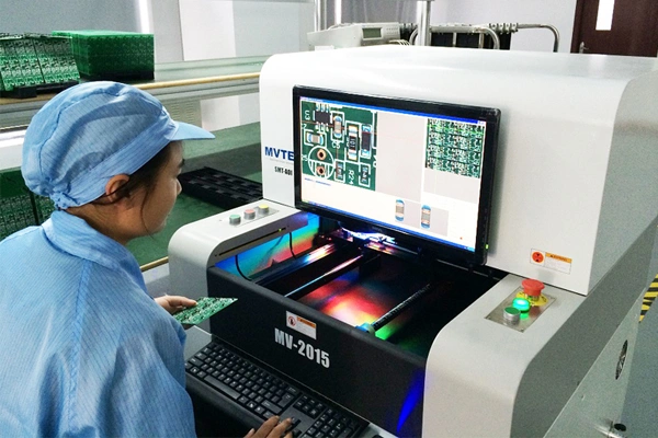
What quality control measures do you have in place for PCB manufacturing?
At JinTeng, we follow stringent Understanding IPC Standards guidelines, alongside our ISO and UL certifications. We also help customers Explore PCB Components so they understand the role each part plays in overall quality.
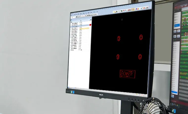
- Automated Optical Inspection (AOI): We utilize advanced AOI systems that use high-resolution cameras to detect defects in the PCB layout and component placement, ensuring precision and accuracy in every board.
- Electrical Testing: Our electrical testing procedures thoroughly verify the functionality of circuits, identifying potential issues like short circuits or open connections to guarantee reliability.
- X-Ray Inspection: For multi-layer boards and hidden solder joints, we employ X-ray inspection to examine internal structures, ensuring all connections are intact and properly formed.
- Functional Testing: We conduct functional testing under real-world operating conditions to evaluate the PCB’s performance, confirming it meets all specified requirements for reliability and durability.
What is the environmental impact of PCB manufacturing process?
At JinTeng, we are committed to minimizing the environmental impact of our PCB manufacturing process through responsible practices and sustainability initiatives:
- Chemical Use: We take great care in managing the chemicals used in processes like etching and plating. All hazardous substances are handled according to strict safety protocols, and we employ advanced technologies to minimize chemical waste.
- Waste Disposal: We ensure the proper disposal and recycling of materials used in the production process. Our waste management systems are designed to prevent environmental contamination and maximize material recovery.
- Energy Consumption: We continuously work on optimizing our manufacturing processes to reduce energy consumption, incorporating energy-efficient technologies where possible to lower our carbon footprint.
- Regulatory Compliance: We strictly adhere to environmental standards and regulations, ensuring our operations meet or exceed local and international environmental guidelines to reduce any negative impacts.
What software do you use for PCB manufacturing?
At JinTeng, we utilize a range of advanced software tools to ensure precision and efficiency throughout the PCB manufacturing process:
- CAD Programs: We use industry-leading design software such as Altium Designer, Eagle, and KiCad to create detailed circuit designs and layouts, ensuring every aspect of the PCB meets our high standards.
- Simulation Tools: To optimize electrical performance and identify potential issues before production, we use sophisticated simulation tools that help verify the design’s functionality and reliability.
- Gerber File Generation: We rely on Gerber file generation software to convert design layouts into formats compatible with our manufacturing equipment, ensuring a seamless transition from design to production.
Which industries utilize your PCB manufacturing services?
- Consumer Electronics: We manufacture PCBs for a variety of consumer devices, including smartphones, laptops, home appliances, and wearables, ensuring high quality and efficiency in mass production.
- Automotive: Our PCBs support critical automotive applications, such as vehicle control systems, infotainment units, and advanced driver-assistance systems (ADAS), with a focus on durability and reliability.
- Aerospace and Defense: We provide high-reliability PCBs for aerospace and defense applications, ensuring performance in extreme environments where failure is not an option.
- Medical Devices: We produce precise and dependable medical PCBs for life-saving equipment, diagnostic devices, and health monitoring systems, meeting stringent regulatory standards and safety requirements.
- Industrial Automation: Our PCBs are used in machinery control, monitoring systems, and automation equipment, delivering the robustness and functionality needed for industrial applications.
What regulations and certifications do you adhere to in PCB manufacturing?
At JinTeng, we adhere to a range of industry regulations and certifications to ensure that our PCBs meet the highest standards of safety, reliability, and quality:
- RoHS (Restriction of Hazardous Substances): We comply with RoHS regulations, limiting the use of specific hazardous materials in our electronic components, ensuring our products are environmentally friendly and safe for use in various industries.
- IPC Standards: We follow IPC standards, which define the quality and performance criteria for PCB design, manufacturing, and assembly, ensuring our products meet the highest industry benchmarks for reliability and functionality.
- UL Certification: Our PCBs are UL certified, demonstrating compliance with safety and reliability standards for a wide range of applications, from consumer electronics to industrial and automotive sectors.
- ISO 9001: We maintain ISO 9001 certification, which focuses on quality management systems and ensures consistent, high-quality production processes throughout our manufacturing operations.
Click here to download all of our Certifications.
What is PCB Manufacturing?
How long does it take to manufacture a PCB?
What is the minimum order quantity for PCB manufacturing?
What resources are available from OurPCB to support my PCB projects?
We offer a variety of articles and guides to help customers better understand PCB technology:
- What is a Printed Circuit Board? — Covers PCB basics.
- Oscilloscope Description and Functions — For testing and troubleshooting.
- Understanding Schematic Diagrams — Interpreting circuit designs.
- Understanding Selective Gold Plating — Surface finishing methods.
- 7 Segment Display Explanation — Component-specific guide.
- PIR Sensor Applications — Motion detection use cases.
- Comparing Fast and Slow Blow Fuses — Fuse types and protection.
- Understanding Tombstoning in Electronics — Common soldering defect.
Can you help with beginner projects or simple circuit builds?
Does OurPCB offer manufacturing and assembly under one roof?
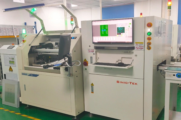
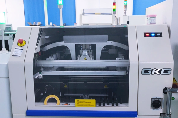
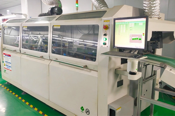
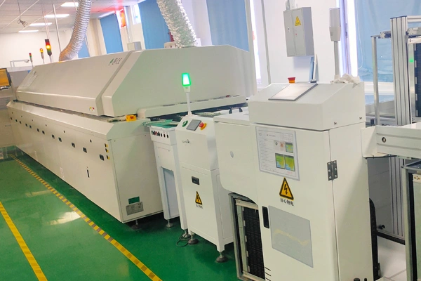
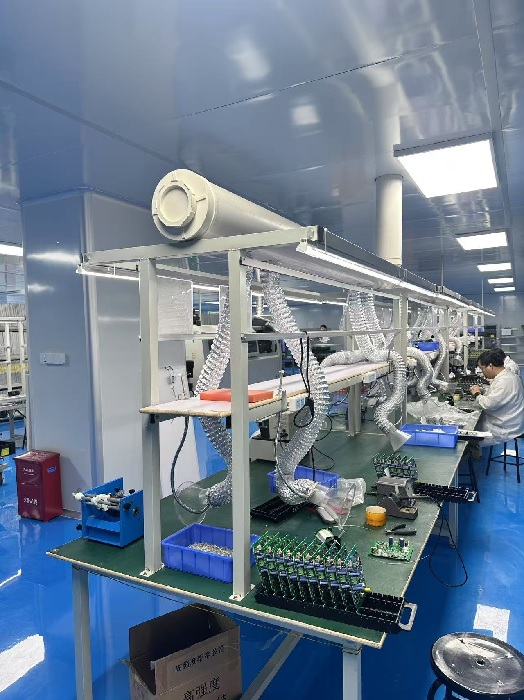
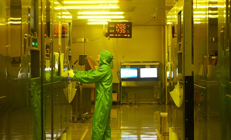
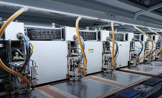
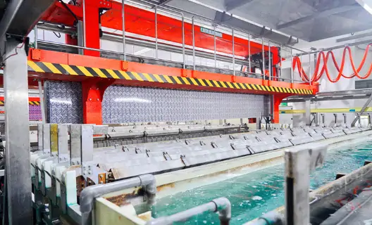
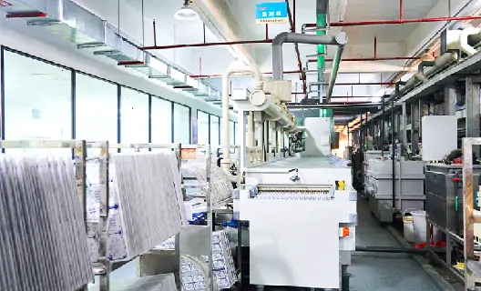
What we factory
Electronic Manufacturing Factory