Quality

JinTeng emphasizes the point that top quality does not only come from stringent production but also from a scientific, open monitoring system. Quality assurance is achieved in the best way through lean management and meticulous attention to detail. Contrary to the other EMS companies, we precisely concentrate on major processes less concentrated on by others. These processes cut through the whole PCBA fabrication process. We are not merely a PCBA service provider but your reliable manufacturing partner for product development. Our ability to stand out as one among many PCBA companies rests precisely on our rigorous quality control process and its strict enforcement.

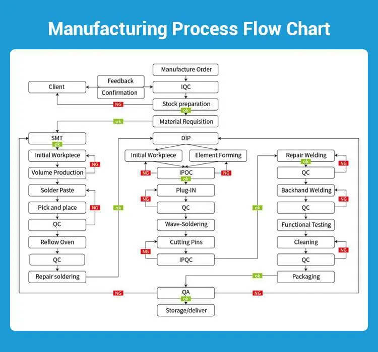
We firmly believe that exceptional quality stems from forward-thinking design and precise control throughout the entire process, not merely final inspections. Therefore, we employ a unique “Critical Process Quality Control Mechanism” to focus monitoring and enforce strict management on core processes that directly impact final product performance yet are often overlooked. From design to delivery, we maintain vigilance over every potential quality-impacting step to ensure absolute reliability.

PCB Quality Control Methods in JinTeng

We at JinTeng utilize a diversified inspection methodology to establish a multidimensional monitoring system that can accurately determine and locate a number of possible defects. We formulate best quality control solutions for various production volumes and product types.

For electrical performance testing, we employ high-speed In-Circuit Testing (ICT) and flexible flying probe testing to provide true confidence with varying production volumes. ICT applies test probes to touch test points on printed circuit boards, with automatic scan to detect open circuits, short circuits, and erroneous component values with very high speed and accuracy in high-volume manufacturing. For prototype or low-volume production, flying probe testing offers the same precision with programmed movement of the probes – eliminating costly specialized fixtures and making it the ideal choice for quick verification and cost savings.

We employ high-resolution Automated Optical Inspection (AOI) to capture PCB images for visual and internal structure examination. We detect cosmetic errors such as misplaced parts or solder joints with the use of such images against schematics. To detect ultra-fine pitch, high-density PCB internal flaws, we utilize X-ray inspection (AXI) to locate concealed faults such as BGA solder void and internal chip cracks in an unobscured manner without destructive teardown. Also, to prevent solder paste print defects, we perform targeted solder paste inspection (SPI).

QC Process Items Checked
IQC
  • PCB: Thickness, vias, pads, silkscreen, warping degree, circuits, solder mask, etc;
  • Components: Part-number, quantity, value, RoHS, appearances, solder pins, temperature resistance, etc;
Storage
  • Sensitive components: stored in a relative humidity 5% cabinet;
  • RoHS Compliant: labeled with RoHS or Non RoHS remarks after IQC process;
  • Solder Paste Application: sealed and stored in a 2-10℃ refrigerator, labeled with expiration date;
  • Material identification card;
Solderpaste
  • Choosing famous solderpaste brands like ECO, Alpha, Vital;
  • Applying automatic solder paste mixing machine to stir clockwise for 2–5 minutes until the solder paste reaches a filamentous state and immediately use for production;
  • Using famous brand laser stencil and paying highly attention to the high precision solder pads like BGA, QFN, etc;
  • Controlling solderpaste thickness, area, volume distribution with 3D SPI Inspection and non-contact laser 3D scanning intensive sampling technology;
SMT Soldering
  • Having 8 automatic Pick & Place production lines with Samsung SM471/482/481, Fujifilm CP8/6 series, electric feeders;
  • Supporting common IC, BGA, QFN, PLCC, and other components of precision package components assembly;
  • Having a reflow oven with 10 temperature zones to leave more time for solderpaste melting and solidification, making sure the temperature rising and dropping more steadily;
  • Using AOI detection at the end of every production line to automatically scan PCB through the camera and collect images to compare the actual solder joints with the qualified images in the database;
  • Having X-ray inspection equipment to check the soldering quality for BGA assembly;
  • Conducting the first article inspection before running the rest of production;
Assembly Inspection
  • Maintaining real-time communication with the client to translate all instruction requirements for the engineer;
  • Training and guiding the testers until they can understand all steps and operate independently;
  • Sharing the test operation steps and test results with the customer through a video record for confirmation and archiving;
  • Proceeding with 100% products after the test result is confirmed by the client;
  • Recording failure test results and informing how to resolve them and as a basis for future design improvements;
Package Carefully packing PCBA board with bubble bags, pearl cotton, electrostatic bags, and vacuum bags before transportation to prevent damage caused by static and crushing;

Prior to product delivery, we perform Functional Circuit Test (FCT) to simulate actual-use conditions in real life. This tests the functionality of each circuit board module to ensure that all functions conceived, including power management, signal processing, and logic control, are met to maximum capability. For long-term reliability, we establish dedicated testing environments for ageing and environmental stress tests. PCBs are subjected to continuous exposure to specific temperatures, humidity, and vibrations to actively identify and eliminate potential defects, assuring the products delivered to you offer superior reliability and endurance.

Also, we perform rigorous solderability testing to examine the soldering capability of PCB surfaces, minimizing cold solder joints and solder voids at the beginning. Contamination testing ensures surface purity, eliminating corrosion and electrical failure from ionic contaminants. On high-speed or high-frequency PCBs, Time Domain Reflectometry (TDR) is utilized to rapidly detect faults like open circuits and shorts. Parallel to this, peel tests determine substrate and copper foil bond strength entirely to safeguard the mechanical stability of the PCB.

Supplier Qualifications

JinTeng understands the importance of long-term service for customers. Who wants to frequently change suppliers? Due to our uncompromising focus on quality and customer satisfaction, we have established long-term relationships with 7 large customers, with annual orders exceeding 15 million US dollars. In order to provide our customers with the necessary trust and assurance in the quality of our products, we follow internationally accepted practices and adopt authoritative standards. Our certifications include:
  • ISO 9001: This standard provides the basis for developing a Quality Management System (QMS) to help organizations ensure that their products and services meet customer needs and continuously improve their business processes.
  • ISO 14001: This standard is used in the establishment and implementation of Environmental Management Systems (EMS). It aims to help companies reduce their adverse impact on the environment while realizing economic benefits and fulfilling social responsibilities.
  • ISO/TS 16949: This standard is developed by the International Automotive Task Force (IATF) for the establishment and implementation of a QMS for the automotive industry supply chain. It is a supplement and extension of ISO 9001 and aims to help automotive industry organizations achieve best practices in quality management, continuous improvement, and supply chain management.
  • ISO 13485: This international standard is for QMS in the medical device industry. It is designed to help medical device industry organizations ensure that their products meet customer and regulatory requirements.

Precision PCB Quality Assurance Throughout the Entire Process

Our quality assurance permeates every stage of PCB design, manufacturing, and assembly, forming an impenetrable quality defense.
Quality Control in Design Phase
  • Schematic Design: Through the use of professional design software and utilization of simulation tools to predict circuit performance, we proactively seek out and eliminate problems such as signal integrity and power integrity that lead to functional failure before they become problems.
  • PCB Routing and Layout: Comply with strict design standards to optimize component placement and trace routing. For high-frequency and high-speed circuits, use cautious impedance matching for loss-free, secure signal transmission.
  • Design File Output: Produce completed, flawless Gerber, drill, and BOM files that guarantee error-free transmission of manufacturing data.
PCB Manufacturing Quality Control
  • Raw Material Inspection: Conduct rigorous physical and chemical property examinations of all raw materials – substrates, copper foil, and inks – to ensure total conformity to standards and eliminate source-level quality problems.
  • Process Control: Precisely control process parameters in critical operations like etching, lamination, drilling, and plating. Utilize automated equipment to monitor in real time to achieve process stability and consistency.
  • In-Process Inspection: Employ AOI and AXI technologies to inspect PCBs during the production process, timely detecting circuit faults, hole position deviations, and other issues for early prevention.
Quality Management in Assembly Phase
  • Component Inspection and Screening: Use professional instruments like LCR meters, multifunction testers, and microscopes to inspect all electronic components purchased for appearance, parameter, and performance. Conduct additional screening, like ageing tests for essential components, to ensure only qualified components enter the production line.
  • Solder Paste Pad Inspection: Inspect solder paste thickness, area, and volume using Solder Paste Inspection (SPI); guarantee PCB pad integrity for SMT placement preparation.
  • Placement and Soldering: Employ high-precision placement machines and soldering equipment, with careful control of soldering temperature profiles and pressure for precise placement and robust solder joints. Later visual inspection and electrical testing eliminate faults like cold solder joints and short circuits.
  • Functional Testing: Simulate the PCB’s actual operating environment to conduct comprehensive functional testing. Verify all functions operate normally, ensuring product performance meets design specifications.

Common PCB Quality Inspection Items & Quality Control Standards

Our testing encompasses all dimensions, including product appearance, electrical properties, physical characteristics, and reliability, strictly adhering to international and domestic standards.
Appearance and Dimensional Inspection
  • Packagings and Markings: Packagings must be moisture-proof, anti-static, and tamper-proof; markings (model, batch, date of production) must be clear, precise, and permanent.
  • Structure and Dimensions: Verify outer dimensions, board thicknesses, and hole diameters with accurate measurement tools to attain full design drawing compliance.
  • Surface Defects:
    • Circuitry: No open or short circuits, no depressions, no copper residue.
    • Solder Mask: Uniform color, bubble-free, peeling-free, and pinhole-free with proper adhesion.
    • Gold Fingers and Pads: The PCB pads must be solderable and clean; the gold fingers must be scratch-free, free from exposed copper, or contamination.
Electrical Performance Testing
  • Conductivity Testing: Deliver 100% conductivity for all traces and vias intended, with strictly grade-specific standards being achieved by resistance values.
  • Insulation Resistance Test: Test insulation resistance between adjacent traces. Class 2/3 products require ≥2MΩ to prevent signal interference and leakage.
  • Impedance Control Test: For high-speed/high-frequency boards, test characteristic impedance using TDR with precisely controlled deviation of ±10% to ensure signal transmission quality.
  • Solderability Test: Require complete solder wetting of pads and vias with a wet zone greater than 95%, ensuring a solid foundation for subsequent assembly operations.
Physical and Process Performance Inspection
  • Board Bend/Warp: Diagonal distortion must be measured, with ≤0.75% required to qualify for flatness for SMT assembly and assembly final.
  • Copper Quality: Conduct microscopic section inspection to verify hole thickness compliance (e.g., minimum average through-hole copper thickness ≥25μm) and delamination or crack detection.
  • Solder Mask Adhesion: Perform the 3M tape test with no peeling observed.
Reliability and Environmental Adaptability Testing
  • Thermal Stress Testing: Simulates the reflow soldering temperatures with a 288℃ solder lift test to ensure panel-to-copper bond strength and heat resistance, with no bubbling or delamination.
  • Temperature Cycling Testing: Conducts cyclic testing by subjecting products to rigorous temperatures (-40℃ to +125℃) to test material fatigue life by expansion and contraction caused by temperatures.
  • Durability Tests: Includes high-temperature/high-humidity storage (85℃/85% RH) and salt spray corrosion testing to ensure stable performance in harsh environments.
Inspection Category Specific Test Items Common Standard References
Visual Inspection Surface defects (scratches, dents), Line defects (opens, shorts, nicks), Hole wall quality, Solder mask coverage, Marking/Legend IPC-A-600, Customer Drawings
Physical/Structural Inspection Dimensions (thickness, length, width), Hole location, Line width/space, Warpage IPC-6012, IPC-TM-650, Customer Drawings
Electrical Performance Testing Continuity Test (Open/Short) IPC-9252, IPC-6012
  Insulation Resistance IPC-TM-650 (2.6.8), IPC-6012
  Withstanding Voltage (Dielectric Withstand) IPC-TM-650 (2.6.7), IPC-6012
Mechanical Performance Testing Peel Strength IPC-TM-650 (2.4.1), IPC-6012
  Solder Pad Strength / Plated-Through Hole Pull Strength IPC-TM-650 (2.4.13, after thermal stress)
Environmental & Reliability Testing Thermal Stress Test (Solder Float or Hot Oil) IPC-TM-650 (2.4.13), IPC-6012
  Solderability Test IPC-TM-650 (2.4.14), IPC-6012
  Ionic Cleanliness (Contamination Test) IPC-TM-650 (2.5.17), IPC-6012
  Thermal Aging, Thermal Cycling, Humidity Testing IPC-6012, IPC-TM-650, GJB 362B
Chemical/Material Analysis Surface Finish Thickness (e.g., Gold, Tin thickness) IPC-4552 Series, IPC-TM-650
  Material Composition (Flammability UL94) UL 94
  Hazardous Substances (RoHS Compliance) IEC 62321

Independent and Comprehensive PCB Quality Management System

We have established an independent quality assurance department responsible for the formulation of quality standards, monitoring of production processes, and reviewing quality documents. The department reports directly to senior management to guarantee the independence and credibility of quality operations. A trained quality inspection team with advanced testing equipment conducts meticulous inspections and testing of raw materials, semi-finished goods, and finished products.

We always adhere to the principles of quality improvement and continuous optimization, taking strong measures of quality enhancement. It encompasses researching and documenting quality issues that may arise during production, identifying root causes, and formulating feasible correction actions. With continuous refinement of production processes, improving quality control procedures, and improving employee quality awareness, we constantly elevate product quality and production efficiency.

Our detailed quality test report system provides meticulous documentation of minute information from every apparatus test, including basic details, visual inspection results, dimensional measurement information, electric performance test data, material and process inspection findings, types of defects, and recommended measures. This enables complete traceability and transparency in quality assurance.

Quality is the foundation of everything we do. Across all JinTeng facilities, strict quality controls and industry certifications ensure that every PCB assembly meets the highest performance and compliance standards.

Quality Policy

JinTeng is dedicated to delivering high-performance electronic manufacturing solutions that meet or exceed customer expectations for quality, reliability, and compliance.

We achieve this by maintaining robust quality systems across all facilities, embracing continuous improvement, and empowering our teams through ongoing training and development. Our commitment to excellence is reflected in every PCB assembly we produce — from prototypes to full-scale production.

This quality policy is more than a statement — it is a shared responsibility. We ensure it is diligently followed by every team member across the Foxtronics group, guiding our actions and decisions to uphold the highest industry standards.

Certifications